New technology milestones and strategic vendor agreement with MACOM position Ayar Labs to lead in multibillion-dollar opportunity for data-intensive workloads within artificial intelligence, high performance computing, cloud, telecommunications and aerospace.
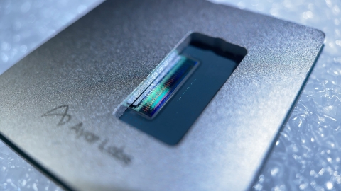
Ayar Labs announced today that it has successfully demonstrated the industry’s first Terabit per second Wavelength Division Multiplexing (WDM) optical link with its TeraPHY™ optical I/O chiplet and SuperNova™ multi-wavelength optical source. The demonstration shows a fully functional TeraPHY chiplet with 8 optical ports running error free without Forward Error Correction (FEC) for a total bandwidth of 1.024 Tbps and at less than 5 pJ/bit energy efficiency. This is a major milestone in providing optical connectivity to meet the ever-growing bandwidth needs of data-intensive applications, low power interconnects, and new innovative heterogeneous and disaggregated system architectures.
This press release features multimedia. View the full release here: https://www.businesswire.com/news/home/20210608005541/en/

Ayar Labs TeraPHY(tm) optical I/O chiplet (Photo: Business Wire)
“This is yet another industry first demonstration of our technology which promises to transform computing and extend the benefits of Moore’s Law,” said Charles Wuischpard, CEO, Ayar Labs. “Digital transformation is being driven by cloud, connectivity, artificial intelligence, and intelligent edge; our roadmap of products and custom solutions is tailored to serve these high-volume market segments. We remain on track to deliver on several customer commitments by end of year.”
Ayar Labs also demonstrated the industry’s first multi-wavelength, multi-port optical source with 64 addressable wavelengths. Named SuperNova, it offers eight times the number of wavelengths compared to today’s commercially available pluggable products. The SuperNova is also the first product compliant with the optical source specifications of the CW-WDM MSA, an industry consortium that drives standards for advanced optical communication and computing applications that require a leap in performance, efficiency, cost, and bandwidth scaling. The multi-wavelength source leverages laser technology from MACOM, a leading supplier of lasers and optoelectronics for telecommunications and data center applications.
“MACOM’s novel laser arrays are ideal for silicon photonics and co-packaged optics,” said Stephen G. Daly, President and CEO of MACOM. “As a promoter-level member of the CW-WDM MSA, we are excited to collaborate with Ayar Labs on the next generation of optical devices based on the MSA’s new specification.”
“Co-packaged optics is expected to transform our industry throughout this decade, by enabling drastic reductions in the cost and power consumption of optical I/Os. Demonstration of a Terabit link is an important step in this direction,” said Vladimir Kozlov, CEO, LightCounting.
The details of this industry-first demonstration will be presented as a postdeadline paper by Dr. Mark Wade, Co-Founder and CTO of Ayar Labs, on Friday, June 11 at 9:15 a.m. PDT at the Optical Fiber Communication Conference (OFC) 2021. OFC postdeadline papers represent the latest and most advanced technical achievements in the field.
Additional Resources:
- OFC postdeadline paper: An Error-Free 1 Tbps WDM Optical I/O Chiplet and Multi-Wavelength Multi-Port Laser (F3C.6) (available via OFC conference web site for registrants)
- Video demonstration: Ayar Labs SuperNova 64 wavelength optical source
- Press release: CW-WDM MSA Consortium Releases New Specification for Multi-Wavelength Optical Laser Sources
About Ayar Labs
Ayar Labs is disrupting the traditional performance, cost, and efficiency curves of the semiconductor and computing industries by driving a 1000x improvement in interconnect bandwidth density at 10x lower power. Ayar Labs’ patented approach uses industry standard cost-effective silicon processing techniques to develop high speed, high density, low power optical based interconnect “chiplets” and lasers to replace traditional electrical based I/O. The company was founded in 2015 and is funded by a number of domestic and international venture capital firms as well as strategic investors. For more information, visit www.ayarlabs.com.
View source version on businesswire.com: https://www.businesswire.com/news/home/20210608005541/en/
Contacts
Kristine Raabe, media@ayarlabs.com


